Data Source: Mitsubishi
The MC Data Source connects directly to the Mitsubishi Q/L Series PLCs using the MELSEC Communications Protocol (MC) to read and write PLC device memory locations.
This driver has been developed specifically for model L26CPU. While it should work for other models, it is not guarantee that address ranges will work for another model.
Create a new Data Source
A Data Source can be defined in Sym3, right click on Project Explorer > Data Sources then select ‘MC’ from the ‘New Source’ menu.
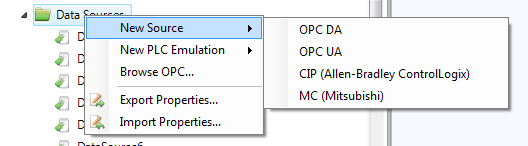
Note: Browsing is not supported for MC Data Sources.
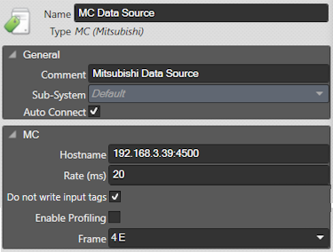
Fill in the IP address or hostname of the PLC in the Hostname field along with the port number that has been created on the PLC for MC service. The port number is required and there is no default. The format is $host:$port.
Examples:
192.168.3.39:4500
mitsubishi1:4500
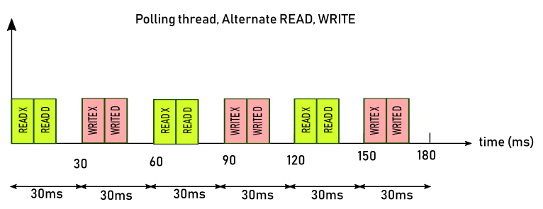
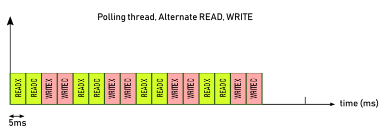
The ‘Update Rate’ is the value in milliseconds between two commands (READ or WRITE). This driver will READ and WRITE alternatively. The image below shows how the update rate is working.
Do Not Write Input Tags
Do Not Write Input Tags is an Integrator-only flag on the Mitsubishi data source that defaults to off.
When enabled, that data source will only write the output tags to the PLC or emulator that it is connected to.
Note: Reads and writes for bit devices (like X and Y) are always aligned to 16 bit alignment. Take for example, the X device:
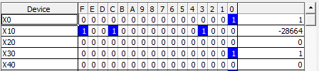
If tags X0 through XE are output tags, and XF is an input tag, XF will be written even if Do Not Write Input Tags is enabled. Same goes for X10 through X1F, X20 through X2F, and so on.
An address that is associated with multiple tags will only be considered an input tag if all the tags are input tags. Consider an example where a project has three tags pointing at D0:
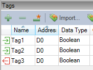
D0 will always be written, as Tag3 is an output tag.
Examples
Example 1
A project with 200 tags using the D register. D0 through D99 are output tags, and D100 through D199 are input tags.
| Addresses | IO Direction |
|---|---|
| D0,D1,D2,…,D99 | Output |
| D99,D100,…,D199 | Input |
If Do Not Write Input Tags is enabled, there will be one write command for the D register, writing D0 through D99, for every write cycle. No additional write commands for D registers 100 through 199 shall be emitted, as they are input tags. If Do Not Write Input Tags is disabled, there will be one write command for the D register, writing D0 through D199, for every write cycle.
Do Not Write Input Tags Disabled
| Command | Range |
|---|---|
| Read | D0 to D199 |
| Write | D0 to D199 |
Do Not Write Input Tags Enabled
| Command | Range |
|---|---|
| Read | D0 to D199 |
| Write | D0 to D99 |
Example 2
A project with 200 tags using the D register in the following arrangement: D0-D49:output,D50-D99:input,D100-D149:output,D150-D199:input.
| Addresses | IO Direction |
|---|---|
| D0,D1,D2,…,D49 | Output |
| D50,D51,…,D99 | Input |
| D100,D101,…,D149 | Output |
| D150,D151,…,D199 | Input |
If Do Not Write Input Tags is enabled, there will be two write commands per write cycle for the D register. The first writing D0-D49, and the second writing D100-D149. If Do Not Write Input Tags is disabled, there will be one write command for the D register, writing D0 through D199, for every write cycle.
Do Not Write Input Tags Disabled
| Command | Range |
|---|---|
| Read | D0 to D199 |
| Write | D0 to D199 |
Do Not Write Input Tags Enabled
| Command | Range |
|---|---|
| Read | D0 to D199 |
| Write | D0 to D49 |
| Write | D100 to D149 |
Example 3
A project with 200 tags using D register in the following arrangement: D(Even numbers):output,D(Odd numbers):input.
| Address | IO Direction |
|---|---|
| D0 | Output |
| D1 | Input |
| D2 | Output |
| D3 | Input |
| … | … |
| D198 | Output |
| D199 | Input |
If Do Not Write Input Tags is enabled, there will be 100 write commands per write cycle for the D register. The first writing D0, and the second writing D2 and so on until D198. This will significantly reduce performance. If Do Not Write Input Tags is disabled, there will be one write command for the D register, writing D0 through D199, for every write cycle.
Do Not Write Input Tags Disabled
| Command | Range |
|---|---|
| Read | D0 to D199 |
| Write | D0 to D199 |
Do Not Write Input Tags Enabled
| Command | Range |
|---|---|
| Read | D0 to D199 |
| Write | D0 only |
| Write | D2 only |
| Write | D4 only |
| … | … |
| Write | D198 only |
Example 4
| Addresses | IO Direction |
|---|---|
| D5000,…..,D5005 | Input |
| D5100,…..,D5105 | Input |
| D6000,…..,D6005 | Output |
| D6100,…..,D6105 | Output |
| D10000,….,D10005 | Input |
| D10100,….,D10105 | Input |
| D11000,….,D11005 | Output |
| D11100,….,D11105 | Output |
Do Not Write Input Tags Disabled
| Command | Range |
|---|---|
| Read | D5000 to D11105 |
| Write | D5000 to D11105 |
Do Not Write Input Tags Enabled
| Command | Range |
|---|---|
| Read | D5000 to D11105 |
| Write | D6000 to D9999 |
| Write | D11000 to D11105 |
Summary
So long as the input tags are all contiguous, the time between MC commands will be unchanged regardless of whether or not Do Not Write Input Tags is enabled. But with discontiguous tags, the number of write commands will be increased when the box is checked.
Note: When there is no input tag mapped for the device, Sym3 will write everything in one command from minimum to maximum range.
Frame
The ‘Frame’ is the protocol you wish to use when communicating the the PLC device. We support Frame 3E and 4E message formats.
Example of configuration:
Adding a MC Tag
Click on the Property Editor option in the Ribbon bar to open the Property Editor Panel.
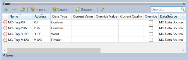
Create Tags in the Tag Manager Window using the + button.
Enter a Name for the Tag in Sym3 and the Data Source for the Tag.
Entering a Data Type for tags is optional. The default will be Boolean for bit devices and Word for word devices. (refer to table below)
The Tag Address is the combination of a 1 to 3 character alphabetic Device Code mnemonic and the numeric address of the Device Point.
Please note that for this Datasource, there’s no ‘Update Rate’ and ‘Simulate Tag’ properties.
By Mitsubishi’s convention, numerical device point addresses are specified in either decimal or hexadecimal radix, specified individually by device with no particular pattern as to which devices use which radix.
Example:
- X10 – Device X, device point sixteen.
- M10 – Device M, device point ten.
- XA – Device X, device point ten.
The table below lists the device codes, type and address radix for the devices supported by the MC data source.
| Device Name | Code | Type | Radix | Address Min | Address Max |
|---|---|---|---|---|---|
| Special relay | SM | Bit | Decimal | SM0 | SM2047 |
| Special register | SD | Word | Decimal | SD0 | SD2047 |
| Input | X | Bit | Hexadecimal | X0 | X1FFF |
| Output | Y | Bit | Hexadecimal | Y0 | Y1FFF |
| Internal relay | M | Bit | Decimal | M0 | M8191 |
| Latch relay | L | Bit | Decimal | L0 | L8191 |
| Annunciator | F | Bit | Decimal | F0 | F2047 |
| Edge relay | V | Bit | Decimal | V0 | V2047 |
| Link relay | B | Bit | Hexadecimal | B0 | B1FFF |
| Data register | D | Word | Decimal | D0 | D143359 |
| Link register | W | Word | Hexadecimal | W0 | W1FFF |
| Timer Contact | TS | Bit | Decimal | TS0 | TS2047 |
| Timer Coil | TC | Bit | Decimal | TC0 | TC2047 |
| Timer Current Value | TN | Word | Decimal | TN0 | TN2047 |
| Retentive Timer Contact | STS | Bit | Decimal | Not Supported | Not Supported |
| Retentive Timer Coil | STC | Bit | Decimal | Not Supported | Not Supported |
| Retentive Timer Current value | STN | Word | Decimal | Not Supported | Not Supported |
| Counter Contact | CS | Bit | Decimal | CS0 | CS1023 |
| Counter Coil | CC | Bit | Decimal | CC0 | CC1023 |
| Counter Current value | CN | Word | Decimal | CN0 | CN1023 |
| Link special relay | SB | Bit | Hexadecimal | SB0 | SB7FF |
| Link special register | SW | Word | Hexadecimal | SW0 | SW7FF |
| Direct access input | DX | Bit | Hexadecimal | Not Supported | Not Supported |
| Direct access output | DY | Bit | Hexadecimal | Not Supported | Not Supported |
| Index register | Z | Word | Decimal | Not Supported | Not Supported |
| File register - Block switching method | R | Word | Decimal | Not Supported | Not Supported |
| File register - Serial number access method | ZR | Word | Hexadecimal | Not Supported | Not Supported |
Device Types and Data Conversions
Sym3 supported data types:
- Default
- sBoolean
- Char
- Byte
- Short
- Word
- Long
- DWord
Conversions
The Mitsubishi Q/L Series PLCs devices are either of 2 fundamental data types, bit or 16-bit word.
When code in the PLC generates 32 or 64 bit values in word device memory, occupying 2 or 4 device points respectively, the values are ordered in little-endian format and addressed accordingly with the lowest device point address being the least significant 16 bits of the larger type.
There is no ability to address or atomically write a single bit to a word device, therefore bit addressing for word devices is not supported.
When converting between the PLC types and the Sym3 types the following rules apply.
Bit Devices
- When reading tag values for any bit device mapped to any of the Sym3 integer types the value of the bit device will be represented in bit 0 of the integer with the remaining bits having the value of zero.
- When setting tags, for any integer Sym3 type, the bit device will be set with the value from bit 0 of the integer and all other bits ignored.
Word Devices
- When reading or writing tag values for any word device mapped to a Sym3 Boolean type the data is read from or written to bit 0 of the addressed device point.
- When reading or writing tag values for any word device mapped to a Sym3 Byte or Char type the data is read from or written to bits 0-7 of the addressed device point.
- When reading or writing tag values for any word device mapped to any of the Sym3 integer types the usual rules apply for the promotion and demotion of integer types.
- When reading or writing tag values for any word device mapped to any of the Sym3 32 or 64 bit integer types the address of the data is the lowest device point word address.